
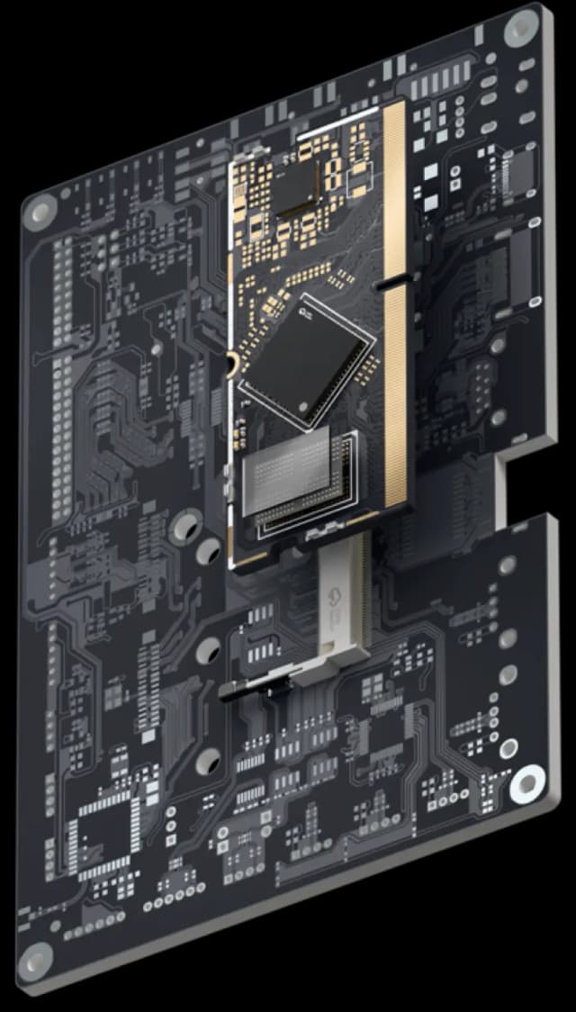
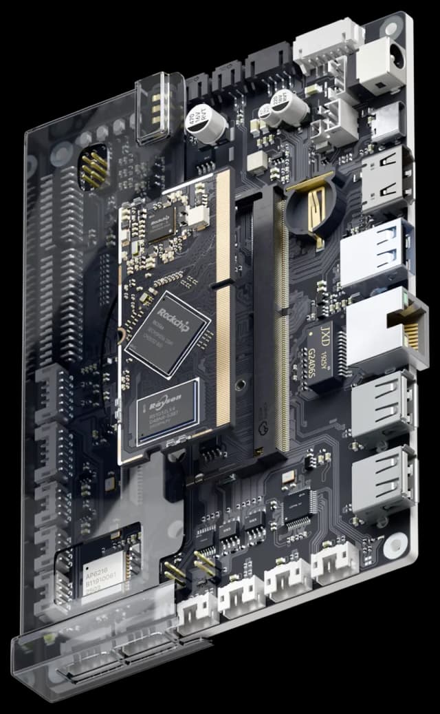





PCBA Testing Decision Guide: ICT vs. FCT vs. Boundary Scan vs. Flying Probe
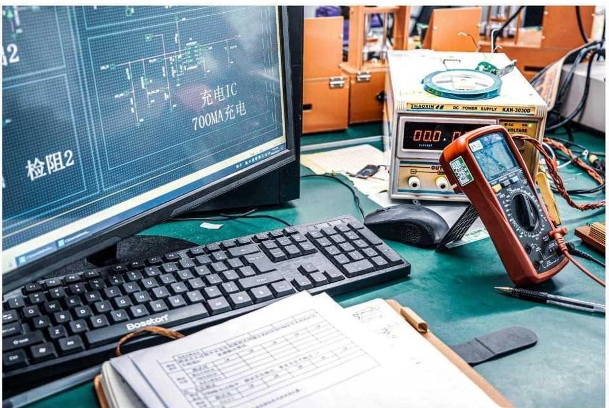
Compare test coverage, fixture costs, turnaround times, and defect detection capabilities to choose the optimal testing matrix (ICT vs. FCT) for your board.
Meet ChipPCBA Global Engineering Team | Hall C3 Booth 168
High-precision fabrication and assembly capabilities certified to IPC Class 3, ISO 9001, and IATF 16949 standards.

Standard & advanced rigid PCBs with industry-leading 24-hour turnaround.

Turnkey PCBA from component procurement to final surface mount assembly.

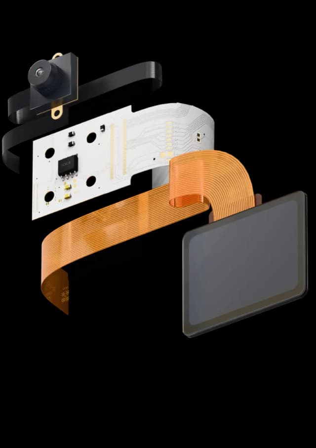
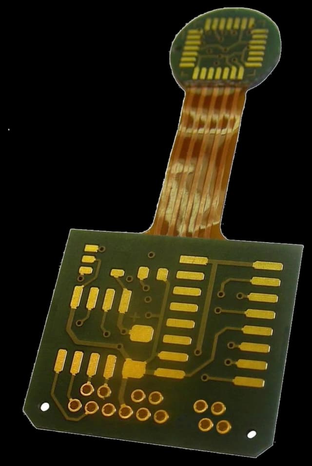
Single to multilayer flexible printed circuits engineered for tight spaces.

Hybrid boards eliminating connectors and cables for mission-critical hardware.

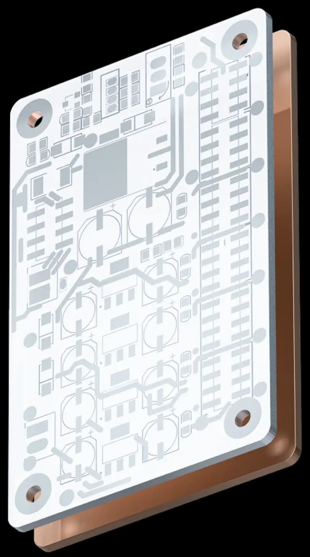
Metal core PCBs designed for maximum heat dissipation in high-power systems.
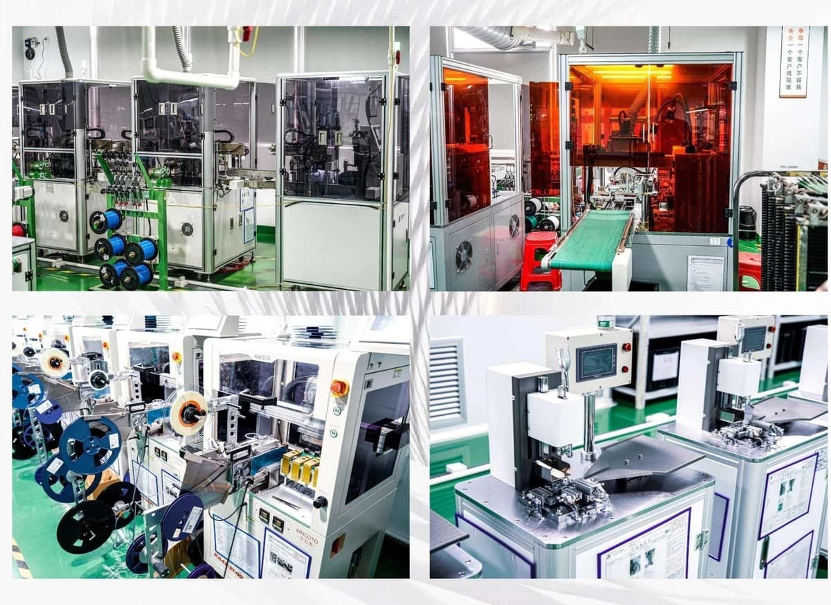
Spanning over 800,000 m² across specialized manufacturing centers, ChipPCBA integrates industry-leading German, Japanese, and Korean automation to deliver aerospace-grade precision and uncompromised PCB/PCBA reliability.
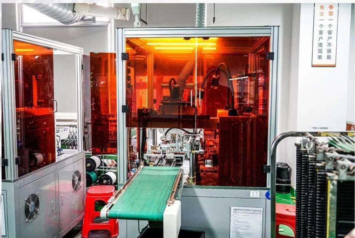
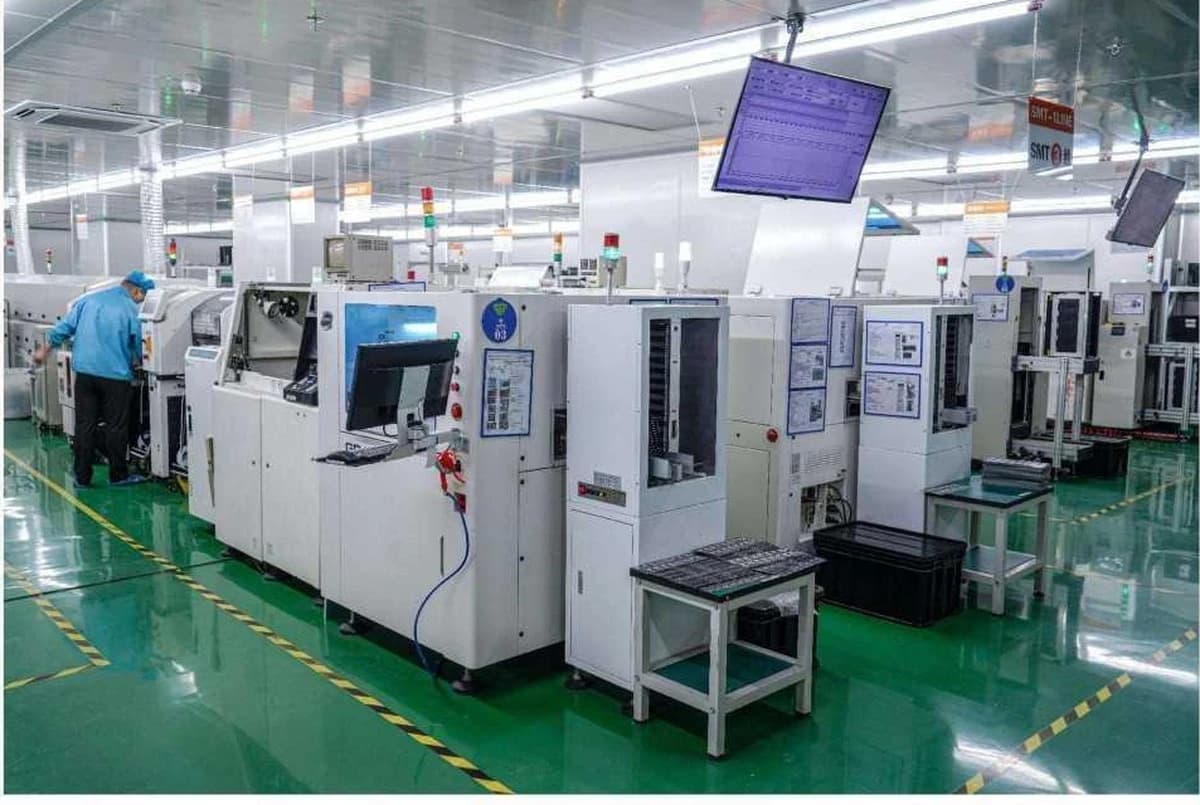
Witness high-speed Panasonic SMT, 3D SPI/AOI & LPKF Laser microvia drilling
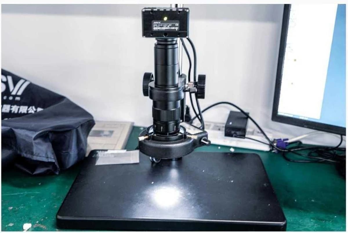
Precision hardware guarantees micrometer-level accuracy on every batch

High-precision UV/CO2 dual-source laser drilling for advanced HDI blind and buried vias with zero burr and thermal stress.

High-speed automated modular pick-and-place lines running up to 100,000 CPH with optical laser centering and dual-lane flexibility.

True 3D shadow-free measurement of solder paste volume, component coplanarity, solder bridging, and tombstoning defects.

Precision electromagnetic solder nozzles in pure nitrogen atmosphere, eliminating thermal damage to adjacent SMD components.

Strict particulate-free cleanroom environment with HEPA filtration, anti-static ESD epoxy flooring, and real-time climate monitoring.

End-to-end digital MES 4.0 system linking CAD files, reel barcodes, reflow profiles, and automated testing results across all plants.
End-to-End Electronics Manufacturing & Engineering Services
Industrial, automotive, and aerospace grade rigid printed circuit boards engineered to withstand high thermal loads and demanding operational environments.
End-to-end PCBA covering surface mount (SMT), through-hole (THT), box-build, and firmware burning with zero minimum order quantity requirement.
Comprehensive PCB layout design and signal integrity engineering assistance to accelerate hardware prototyping and ensure first-pass success.
Industry-standard manufacturing feasibility analysis software that identifies assembly risks, clearance conflicts, and design traps before fabrication.
Direct franchise procurement network with smart warehousing, guaranteed authenticity, full lot traceability, and competitive volume pricing.
Trusted by over 300,000 hardware engineers and global enterprises across 166 countries for high-precision, mission-critical electronics manufacturing.
Real feedback from engineers prototyping and scaling products worldwide
“ChipPCBA delivered our 10-layer Rogers high-frequency hybrid boards in just 4 days. The trace impedance and dielectric consistency were flawless, easily passing all laboratory RF measurements.”
Senior Hardware Engineer • RoboDrive GmbH
“The turnkey assembly service is exceptional. Their CTDFM software caught an 01005 footprint conflict before manufacturing, saving our team at least two weeks of re-spinning prototype boards.”
Principal Embedded Architect • AeroDynamics Labs
“From component procurement to X-Ray BGA inspection, ChipPCBA provides military-grade consistency. We have placed over 80 orders with zero defect reports. Outstanding build quality.”
Lead Power Electronics Designer • EcoMotion Tech
“Our satellite IoT communication payload required high-density interconnect rigid-flex boards. ChipPCBA delivered exceptional ENIG surface finishes and zero-impedance deviance across thermal cycling.”
Head of Hardware Systems • AeroPulse Avionics
“Assembling micro-BGA components with 0.3mm ball pitch for surgical robotic arms is challenging. Their 3D SPI and X-Ray inspection reports gave our medical regulatory team total peace of mind.”
Robotics Research Director • NeuroMotion Systems
“Their heavy copper 4oz boards withstand our extreme Scandinavian winter temperatures effortlessly. Heat dissipation design suggestions from their DFM team reduced our operating thermals by 12°C.”
Chief Technology Officer • Nordic Grid Power
“ChipPCBA's turnkey sourcing eliminated all supply chain headaches. Their automated BOM matching found exact lifecycle-active equivalents with full traceability certificates for our quantum instrumentation.”
VP of Hardware Engineering • QuantumFlux Dynamics
“We subjected their 12-layer HDI radar-sensor boards to AEC-Q200 automotive reliability testing. Zero micro-via delamination and 100% IPC Class 3 compliance across 50,000 production units.”
Senior Autonomous Driving Architect • HyperDrive Mobility
“In sub-nanosecond timing devices, trace length matching and via impedance are everything. The board stackup tolerances from ChipPCBA matched our simulation within 1.5%. Truly Swiss-grade precision.”
Precision Instrumentation Lead • Chronos Scientific
“Speed to market determines our survival in computer vision cameras. ChipPCBA delivered fully populated SMT prototypes in 72 hours, helping us close our Series B evaluation ahead of schedule.”
Founder & CTO • Argos Optics & AI
“Our agricultural robots operate in intense dust and 45°C heat. ChipPCBA's conformal coating and rigorous AOI ensure our telemetry and motor driver modules never drop a packet.”
Director of Systems Engineering • TerraAgri Robotics
“Their cleanroom SMT line handled our biocompatible implantable sensor boards with zero contamination. The turnkey procurement and fast air-express delivery to Singapore was completely seamless.”
Principal Hardware Architect • SingaBio Devices
End-to-end manufacturing, custom payment terms, dedicated account managers, and rigorous global compliance designed to scale with enterprise operations.
Dedicated multilingual teams in North America, Europe & Asia-Pacific ensuring 24/7 round-the-clock engineering response, local time-zone alignment, and rapid quotation turnaround.
Every enterprise client is paired with a designated senior account manager and lead engineer with direct phone, WhatsApp & Teams access for guaranteed < 1h rapid response.
Tailored credit facilities for qualified enterprise partners, OEMs, and academic institutions, supporting Net 30/60 Days and Net 90 payment terms with multi-currency settlement.
Transparent manufacturing process supporting third-party audits by SGS & TÜV, on-site client inspections, or remote high-definition video inspection with full MES traceability.
Dedicated climate-controlled warehouse buffers for customer consignment buffer stock, strategic long-lead components, and direct integration with authorized distributors.
ChipPCBA manufacturing bases adhere strictly to international manufacturing codes, environmental directives, and industry audit protocols.
Standardized quality control from raw material receipt to final dispatch
Rigorous defect prevention, APQP, and PPAP level documentation
Strict cleanroom assembly, traceability, and medical risk mitigation
Flammability and electrical safety verified under File E356494
100% lead-free, halogen-free, and heavy metal compliant processes
Substances of Very High Concern (SVHC) compliance certification
Certified workmanship standards for commercial and high-reliability aerospace products
Unlock dedicated account management, Net 30/60 flexible payment terms, priority SMT production slots, and verified factory audit access.
Experience the peace of mind of having a direct engineering hotline and assigned account manager working side-by-side on your projects.

Specializes in high-mix low-to-medium volume turnkey assembly and rapid turnaround NPI projects for North American IoT and hardware tech startups.

Over 14 years resolving complex PCB layer stackup challenges, 32-layer impedance matching, HDI microvia reliability, and DFA clearance optimizations.

Directs enterprise accounts across Germany, UK, and Europe, specializing in automotive PPAP Level 3 documentation, medical device qualification, and volume pricing.

Leads component engineering and authorized global supply chain pipelines, assisting customers with BOM scrubbing, lifecycle risk alerts, and alternative part validation.
Connect directly with our lead DFM engineers and dedicated sales directors. Free 30-minute design review for multi-layer PCBs and turnkey assemblies.
Explore in-depth DFM guidelines, high-speed PCB stackup engineering, assembly best practices, and ChipPCBA corporate announcements.
Compare test coverage, fixture costs, turnaround times, and defect detection capabilities to choose the optimal testing matrix (ICT vs. FCT) for your board.
Seamlessly import verified design rule constraints and high-frequency stackups into KiCad 8.0 with zero manual parameter setup error, guaranteeing fabrication compatibility.
Essential solder paste aperture ratios, pad land patterns, solder mask dam clearances, and thermal relief design for 0.25mm Pitch BGA and ultra-fine pitch components.
Join the global hardware developer challenge to build next-generation CM4 carrier boards with $20,000+ in manufacturing vouchers and prizes for innovative IoT applications.
In-depth guide to microstrip and stripline geometry, dielectric constant variance, return path continuity, and Differential Pair Routing for 10Gbps+ signals.
Highlights and technical presentations from Bochum, Germany showcasing 32-layer backplanes, embedded passive components, and optical inspection methodologies at KiCon Europe.
Engineering standards for CubeSats, lunar landers, and deep-space probes: NASA SP-R-0022A outgassing limits, Sn-Pb alloy exemptions for whisker prevention, and cryogenic solder ductility down to 4 Kelvin.
Direct KiCad 9.0 Plugin and Content Manager (PCM) integration enables real-time DFM clearance auditing, verified stackup imports, and instant quote generation inside the EDA canvas.
Step-by-step methodology for replacing multi-thousand-pin fine-pitch BGAs with cured underfill: localized bottom-board IR preheat, split-vision prism alignment, and non-abrasive pad redressing.
Enterprise rollout of Tin-Bismuth (Sn-Bi) low-temperature soldering across production lines, cutting reflow thermal stress by 50°C and factory energy consumption by 35% with full RoHS 3.0 certification.
Critical guidelines for automotive radar and sub-THz imaging hardware: Rogers RO3003 vs. Megtron 8, substrate-integrated waveguide (SIW) vias, and nickel-free surface finishes.
Successful audit by TÜV SÜD confirms ChipPCBA meets the most rigorous ISO 13485:2026 and FDA 21 CFR Part 820 medical device manufacturing standards.
Get monthly DFM guidelines, high-speed routing whitepapers, component sourcing alerts, and early access to ChipPCBA design contests straight to your inbox.